Two weeks of projects: Day 1
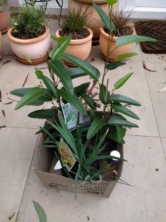
After the leaving drinks and a big sleep-in it was a bit of a slow start. The garden got the first bit of attention — a pair of Hardenbergias to grow up the pergola outside.
Then we spent a bunch of time looking at shelves for under the stairs. In the end we found a perfect unit which I’ll install during the week. Progress! Looking forward to getting all the books sorted out.
Google Play helpfully emailed me to tell me that the next season of Orphan Black has started, so we had a quick distraction.
I spent the rest of the evening working on the CPU design. I think I’m pretty happy with the result — 8-bit registers and ALU, 16-bit addressing, Harvard architecture. 6 registers, plus an 8-bit input port and an output port. I’ve got a kind of primitive memory-mapped DMA display. Looking like 26 CPLDs, plus a RAM and ROM chips at this stage. 4-clock pulses per cycle, one instruction per cycle.
I’ve finished the instruction set and the instruction encoding. Next up to write both an instruction-level emulator and a signal-level simulator and start implementing the various blocks on an FPGA.
Some more background on the CPU — this would of course be a lot simpler to do entirely in a simulator, exactly like we did at university. Or even entirely in a single FPGA. The idea here, however, is to make something understandable and usable in a teaching environment. Each individual CPLD is a basic concept — e.g. “4-bit register and bus driver”, “decoder”, “clock generator” or (the big one) “ALU”. In fact, it should be possible to do the VHDL entirely in schematic mode in ISE — so you can start from a gate-level diagram, and work up through the layers to the entire CPU.
The first inspiration for this project is The Mega Processor. It’s just wonderful — take the time to read the entire site… my favourite quote is “This could be where the conflict in scale between the megaprocessor and my living room starts to escalate.”
But I’m not quite that crazy and I don’t like soldering that much, so I found this 4-bit CPU made entirely from 7400 series chips which was exactly the sort of level of abstraction I was looking for — you can entirely understand or teach the functionality of any 7400 chip in one diagram, and the overall CPU is just sequencing those chips in the right way. The rest, as they say, is just wiring. I originally planned to build exactly this circuit, but finding some of those cold war era 74181 ALU chips proved very difficult, so I started thinking about replicating the 74181 in a CPLD. Which ultimately led to realizing that if you replace all the 7400 chips individually with tailor-made ones you can simplify the overall design considerably without getting away from the “each component is individually understandable” requirement.
I’m excited about the LEDs too — watching every step happen visually would be great for demos. I also like the long-term ability to keep extending the design to add more features — interrupts, variable-length instructions, fewer clock pulses per instruction retired, more hardware support for things like the stack, etc.
My goal is to get it to play Pong…